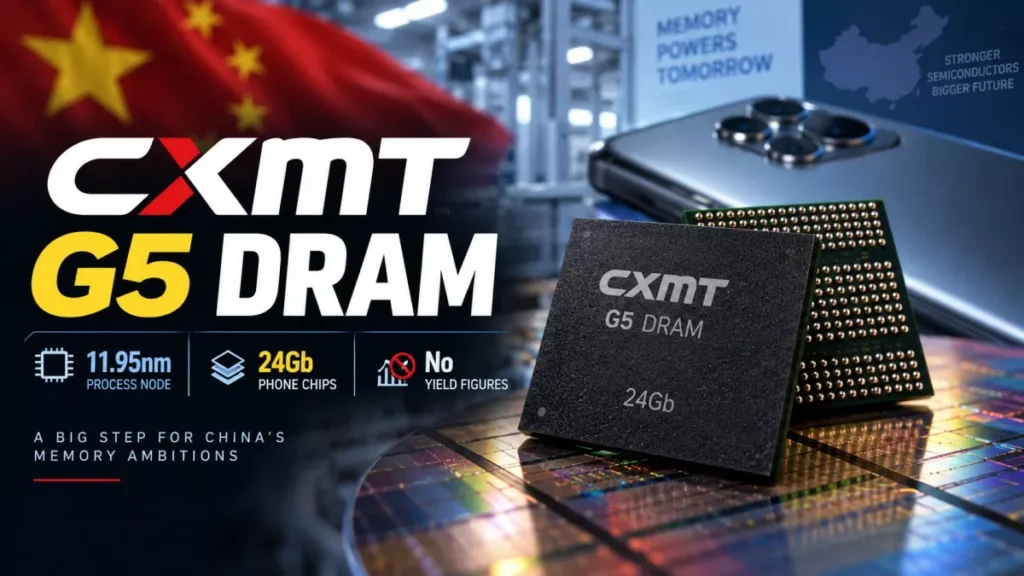

CXMT G5 DRAM entered mass production, the Hefei memory maker announced on 20 September 2026. ChangXin Memory Technologies put the memory array’s active-area half-pitch at 11.95 nanometres and showed two 24-gigabit LPDDR5X phone chips built on the platform. It gave no yield or output figures.
What CXMT Announced in Hefei
CXMT made the announcement at the 2026 World Manufacturing Convention in Hefei, in China’s Anhui province, where it is based. It is China’s largest maker of DRAM, the working memory inside phones, laptops and servers.
Three claims carried the announcement. The G5 platform reaches an active-area half-pitch of 11.95 nanometres in the memory array. It was produced using quadruple patterning, a technique that repeats exposure and etching several times to draw finer features than one pass of the available equipment allows. And, in CXMT’s own words as reported by the South China Morning Post, it delivers “the number of dies produced per wafer increasing by at least 50 per cent from the previous generation while maintaining better energy efficiency and cost control”.
CXMT described the result as close to the level of the world’s most advanced mass-production memory platforms. As of 21 September 2026, that is the company’s own characterisation; no independent laboratory analysis of a G5 die has been published.
What 11.95 Nanometres Actually Measures
The number is not the same kind of number as the node names Samsung Electronics, SK hynix and Micron Technology use, and treating it as one is the easiest mistake to make with this story.
Half-pitch is half the distance between repeating features in the memory array. It is a physical measurement of one specific structure. The “12-nanometre-class” and “10-nanometre-class” labels the three incumbent suppliers apply to their DRAM are marketing generation names, not measurements of the same feature. Analysts cited by the Seoul Economic Daily made exactly this point on the day of the announcement: 11.95 nanometres describes one core structure and is therefore difficult to compare directly with the incumbents’ process names.
What can be said without stretching is narrower. CXMT has moved its own array dimensions down a generation, and it did so with the deep-ultraviolet tools it is allowed to buy.
The Two Chips CXMT Showed
| Item | Detail |
|---|---|
| Product type | LPDDR5X mobile DRAM |
| Capacity | 24 gigabits per die |
| Capacity change | 50% above the previous generation part |
| Packages | 496-ball and 245-ball |
| Stated targets | Mid-range to high-end smartphones and portable consumer electronics |
LPDDR5X is low-power memory designed for battery devices. It is not the server DDR5 or the high-bandwidth memory stacked beside AI accelerators, which matters for the question most readers arrive with. Several outlets reported on 20 September that the two parts are already in mainstream Chinese flagship handsets; CXMT did not name the phone models, and no handset maker has confirmed the parts publicly.
Why This Was Done Without EUV Machines
China cannot buy extreme-ultraviolet lithography systems, which are made almost exclusively by the Dutch company ASML and are blocked by United States and allied export controls. Those controls were built on the assumption that leading-edge DRAM is hard to reproduce without them.
Quadruple patterning is the workaround: rather than printing a fine pattern in one exposure with an EUV machine, the fab prints coarser patterns several times over with older deep-ultraviolet tools and combines them. It works, and it costs more steps, more time and more opportunities for a wafer to go wrong per finished die. That trade-off is the reason the missing yield figure matters. The same constraint shapes China’s wider chip effort, as the Huawei Ascend 960 timeline showed earlier this month.
Where CXMT Now Sits Among DRAM Makers
- Ranking: Fourth worldwide by DRAM revenue, behind Samsung Electronics, SK hynix and Micron Technology.
- Revenue share: 9.5% of global DRAM revenue in the second quarter of 2026, according to TrendForce figures reported by the Seoul Economic Daily; the same firm put CXMT at 7.6% and fourth place in the first quarter.
- Fabs: Three 12-inch plants, two in Hefei and one in Beijing.
- Capacity: Roughly 300,000 wafers a month at present, with reporting pointing to about 350,000 a month by the end of 2026.
The direction is not in dispute. The pace is a matter of reported estimates rather than company disclosure, and CXMT has not published its own capacity numbers. China’s state-backed push to build domestic alternatives runs across the industry, from memory to the planned AI chip clusters.
What It Means for Memory Prices
Nothing announced on 20 September addresses the part of the memory market that has been driving prices up. The squeeze is on server memory and high-bandwidth memory for AI systems, where the three large suppliers have shifted capacity. TrendForce forecast in July 2026 that server DRAM contract prices would rise 13% to 18% quarter on quarter in the third quarter of 2026.
CXMT’s G5 launch products are mobile LPDDR5X sold into smartphones. More supply of phone memory does not relieve a shortage of server memory, and CXMT has not said when or whether G5 will be applied to server DDR5. Analysts quoted by the Seoul Economic Daily expect the AI memory bottleneck to run through 2028. Anyone reading this as news about the price of a desktop RAM kit should treat it as unrelated for now.
What CXMT Did Not Disclose
The announcement left out the numbers that would let anyone judge it. CXMT gave no yield figure for G5, no monthly output for the platform, no pricing, and no timetable for extending it beyond mobile parts. It also did not say which customers are buying the 24Gb chips.
Those gaps are normal for a convention announcement and they are also the whole question. A process that works in a demonstration and a process that fills 300,000 wafers a month profitably are different achievements, and only the second one changes the market.
CXMT G5 DRAM FAQ
What Is the CXMT G5 Platform?
G5 is ChangXin Memory Technologies’ fifth-generation DRAM manufacturing platform. CXMT said on 20 September 2026 that it had entered mass production, with an active-area half-pitch of 11.95 nanometres in the memory array.
Is CXMT Now Level With Samsung and SK Hynix?
No, and the comparison does not work cleanly. The 11.95nm figure measures one structure inside the array, while the incumbents’ “12-nanometre-class” labels are generation names rather than the same measurement. CXMT remains fourth by DRAM revenue.
How Did CXMT Build It Without EUV?
By using quadruple patterning on deep-ultraviolet equipment, repeating exposure and etching steps to reach finer dimensions. EUV lithography systems are subject to export controls that keep them out of China.
Will This Make Memory Cheaper?
Not on the evidence of this announcement. The products shown are mobile LPDDR5X for phones, while the shortage pushing prices up sits in server memory and high-bandwidth memory for AI hardware.
What Did CXMT Not Reveal?
Yields, monthly output for G5, pricing, customer names, and any plan to take the platform beyond mobile memory. Without a yield figure, the cost advantage of the extra density cannot be assessed from outside.